


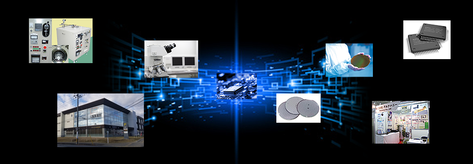
We are a group of technicians for manufacturing equipment.
Ultra-fine
processing of LSI wiring is possible through semiconductor
manufacturing equipment incorporating state-of-the-art technology
The high performance, low power consumption, and low cost of LSI and CPU used in computers, mobile phones, digital cameras, and automobiles has been achieved through the miniaturization of semiconductor integrated circuit processing technology.
The miniaturization of this processing technology has been achieved thanks to the dramatically improved performance of manufacturing equipment.
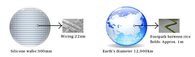
Semiconductor integrated circuits are made by forming a wiring pattern on a silicon substrate with a diameter of 300mm referred to as a wafer. The width of the latest wiring has been shrunk down to the ultra-fine value of just 22nm (=0.000000022m).
If we liken the 300mm wafer to the 12,000km-diameter earth, the latest wiring width would be just 1m or less on the same scale.
All components - mechanical, electrical, and software - of the manufacturing equipment that makes this ultra-fine processing possible are made by bringing together state-of-the-art technology, and an in-depth knowledge and a wide range of experience are required to handle them.
We have many years of experience handling such semiconductor manufacturing equipment.
Our employees consist of excellent technicians with extensive experience at major semiconductor manufacturing equipment manufacturers.
We offer a wide range of services and technology from maintenance and KAIZEN to equipment relocation and start-up, modification, and parts sales.
What is ultra-fine processing? How fine is it?
If we liken the 300mm wafer to the 12,000km-diameter earth, the wiring width would be about the same as the footpath between rice fields on the same scale
Copyright © AlphaNy Corporation All Rights Reserved.